PCB Designer II
El Segundo, CA - USA
Job Summary
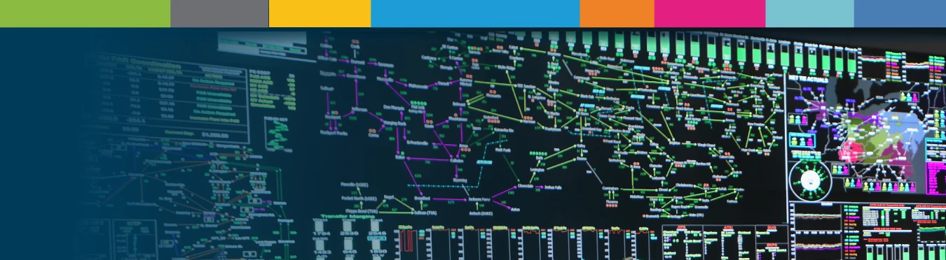
Our boards fly in spacecrafts manage power for fusion systems and process signals in medical devices. Every one of them was designed by someone who owned the layout end to end from stackup definition to manufacturing handoff. This role is for the designer who understands that a great board isnt just electrically correct; its manufacturable testable and built to last.
Role Overview:
As a PCB Designer II you will own the end-to-end design of high-performance printed circuit boards (PCBs) across a variety of applications including power electronics RF mixed-signal and high-speed digital. Youll create schematics develop board layouts and ensure designs meet electrical mechanical and manufacturing requirements. Working closely with cross-functional teams you will drive design decisions anticipate risks and evaluate trade-offs to balance technical performance project timelines and business goals.
What You Will Do:
- Own PCB layouts from concept through manufacturing handoff across power electronics RF mixed-signal and high-speed digital applications
- Apply Design for Manufacturing (DFM) best practices perform design rule checks (DRCs) and interface directly with fabrication and assembly vendors to resolve issues and ensure manufacturing readiness
- Produce consistently high-quality layouts and footprints aligned with IPC standards and SOE best practices
- Identify opportunities to improve PCB design processes libraries and documentation and share lessons learned across the team
- Collaborate with engineers across disciplines to optimize layouts for thermal EMI and mechanical integration
- Inspect incoming PCBAs work with engineering to address footprint or layout issues and feed takeaways back into future designs
What You Will Need:
- Bachelors Degree (Electrical Engineering Computer Science Physics Math related field)
- Hands-on professional experience with professional ECAD tools such as Altium Designer KiCad Cadence PADS etc.
- Demonstrated ability to translate requirements into manufacturable PCB layouts
- Understanding of PCB specifications and properties: stackup & materials trace/space via sizing impedance transmission lines trace capacity & sizing propagation delay etc.
- Excellent written and verbal technical communication skills
- Comfort working across multiple projects adapting to changing requirements and making informed decisions with incomplete information
What Would Be Useful:
- Expertise with Altium Designer or KiCad
- Experience with library configuration management (e.g. Altium Vault database libraries or PLM systems)
- Experience with either high-density high-layer-count or large-format PCB designs preferably for aerospace automotive and/or medical applications
- Experience with HDI stackups: blind & buried vias via-in-pad escape routing of dense BGAs
- Familiarity with IPC and JEDEC standards
- Experience with Git and/or SVN for revision control
Benefits
- Compensation range of $118860-$148580 equity incentive plan
- Flexible work hours and work from home policy
- 100% employer-paid health insurance (Medical Dental Vision) for employees 50% dependent coverage
- Unlimited paid time off policy 11x paid company holidays 12x paid sick days
- 401(k) retirement account and employer matching (Safe Harbor 4%)
- Generous paid parental leave
- Relocation assistance available if 50 miles away from the office
- Electric Vehicle (EV) charging ports
- Catered lunches snacks and accessible kitchen
Our Values in Practice:
SOEs four core values are the standard by which we operate. As a PCB Designer II you are expected to bring them into every layout decision vendor interaction and team dynamic:
- Lead with Curiosity: Question requirements before executing them. Understand why the board needs to perform the way it does and bring what you learn back to the team.
- Own the Outcome: Manage your boards not just your tasks. Communicate early when requirements shift adapt when constraints change and take responsibility for the layout from first footprint to final manufacturing handoff.
- Build the Right Thing: Balance technical rigor with what the project actually needs. Evaluate trade-offs (layer count materials routing density cost etc.) and communicate the implications clearly. Push back when requirements dont match intent.
- Empower Others: Build working relationships across engineering disciplines. Share what you know about layout DFM and vendor constraints proactively. The teams designs get better when you do.
About Second Order Effects:
SOE is an engineering consulting firm that specializes in electrical electromechanical and embedded systems. Founded in 2016 weve grown from a 3-person operation to a team of 40 engineers across offices in El Segundo CA and Redmond that time weve completed over 250 projects for more than 100 clients. Our designs control rocket engines manage satellite communications instrument fusion reactors and are enjoyed by consumers around the world. The only thing we wont build are weapons.
Were 100% employee-owned which means that every engineer at SOE has a real stake in what we build. We structured the company this way because we believe the people best equipped to advance our mission are the ones doing the work.
We approach problems from first principles. We break challenges down to their most fundamental components which is how we find solutions that hold up across industries use cases and engineering functions. We focus on solving the right problems and building the teams to take them on.
Additional Requirements:
- Applicant must be willing to work 40 hours a week on-site in El Segundo California USA
- Applicant must be eligible to work on ITAR projects
- Job Type: Full-time (Salary)
ITAR Requirements:
- To conform to U.S. Government space technology export regulations including the International Traffic in Arms Regulations (ITAR) you must be a U.S. citizen lawful permanent resident of the U.S. protected individual as defined by 8 U.S.C. 1324b(a)(3) or eligible to obtain the required authorizations from the U.S. Department of State. Unfortunately we are unable to provide sponsorship at this time.
If you dont meet 100% of the preferred skills and experience we encourage you to still apply!
Second Order Effects is proud to be an Equal Opportunity Employer; employment with SOE is governed on the basis of excellence and will not be influenced in any manner by race color religion gender national origin/ethnicity veteran status disability status age sexual orientation gender identity marital status mental or physical disability or any other legally protected status.
Required Experience:
IC