Senior Lead Ramp Process Engineer (PVD)
Share
Job Summary
Who We Are
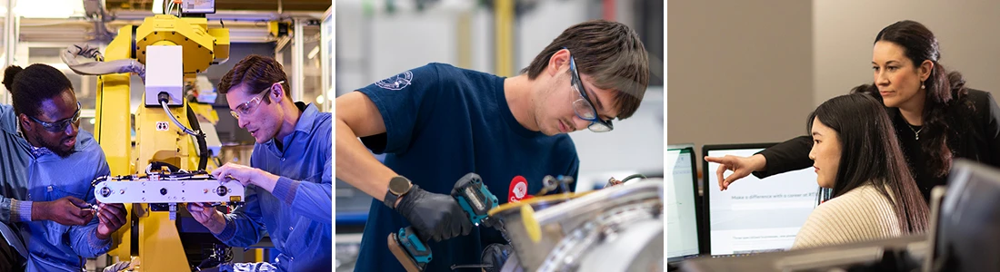
Applied Materials is a global leader in materials engineering solutions used to produce virtually every new chip and advanced display in the world. We design build and service cutting-edge equipment that helps our customers manufacture display and semiconductor chips the brains of devices we use every day. As the foundation of the global electronics industry Applied enables the exciting technologies that literally connect our world like AI and IoT. If you want to push the boundaries of materials science and engineering to create next generation technology join us to deliver material innovation that changes the world.
What We Offer
Location:
SingaporeSGPYoull benefit from a supportive work culture that encourages you to learn develop and grow your career as you take on challenges and drive innovative solutions for our customers. We empower our team to push the boundaries of what is possiblewhile learning every day in a supportive leading global company. Visit our Careers website to learn more.
At Applied Materials we care about the health and wellbeing of our employees. Were committed to providing programs and support that encourage personal and professional growth and care for you at work at home or wherever you may go. Learn more about our benefits.
About Us
Applied Materialsis an innovation-driven company.We are the leader in materials engineering solutions used to produce virtually every new chip and advanced display in the world.Our ability to identify emerging technologies that can complement and leverage Applieds materials engineering expertise is critical to the companys continued growth.
About this role
Looking for a motivated and hands-on Process engineer to support the setup and ramp of our next-generation semiconductor manufacturing this role youll collaborate across engineering and operations to drive smooth technology transfer from pathfinding and ramp to pilot production. Experience and discipline in process transfer to pilot production line will be critical to a successful and efficient fab ramp-up.
Responsibilities:
Review and train on existing R&D processes and transfer knowledge to pilot production line
Create a comprehensive checklist to ensure successful transfer of processes and materials
Collaborate with R&D and production process integration operations and hardware teams to ensure completing the checklist on time to meet timeline needed to start HVM operations
Track and manage schedules deliverables and risks for technology transfer and production milestones.
Coordinate training with R&D transfer engineers
Support tools and process qualifications at HVM site
Qualifications:
Strong understanding of semiconductor manufacturing processes and industry standards including deposition etch lithography and metrology
Comfortable working across time zones collaborating with remote teams and supporting factory-side execution
Discipline tracking and driving deliverables to completion
Flexibility to travel back and forth between South East Asia and the USA (up to 50% of the time)
Work Location:
North
Additional Information
Time Type:
Full timeEmployee Type:
Assignee / RegularTravel:
Yes 50% of the TimeRelocation Eligible:
NoApplied Materials is an Equal Opportunity Employer. Qualified applicants will receive consideration for employment without regard to race color national origin citizenship ancestry religion creed sex sexual orientation gender identity age disability veteran or military status or any other basis prohibited by law.
Required Experience:
Senior IC
Key Skills
- Distributed Control Systems
- Continuous Improvement
- Process Improvement
- Minitab
- Root cause Analysis
- Tooling
- Statistical Software
- Process Engineering
- cGMP
- Programmable Logic Controllers
- Public Speaking
- Manufacturing
About Company

Applied Materials, Inc. is the global leader in materials engineering solutions for the semiconductor, flat panel display and solar photovoltaic (PV) industries.