Principal Process Engineer, Die Bonding
Share
Job Summary
Our vision is to transform how the world uses information to enrich life for all.
Micron Technology is a world leader in innovating memory and storage solutions that accelerate the transformation of information into intelligence inspiring the world to learn communicate and advance faster than ever.
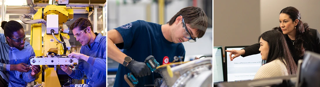
The Advanced Packaging Technology Development (APTD) department at Micron Technology is at the forefront of innovation driving the advancement of memory and storage Interconnects and Packaging solutions that transform how the world uses information. Micron is dedicated to developing innovative processes and technologies that enable the creation of next-generation semiconductor products which drive the AI revolution. By collaborating closely with our global R&D equipment and materials suppliers and manufacturing teams we ensure the efficient development transfer and implementation of new technology nodes maintaining Microns leadership in the industry.
As a Principal Process Engineer in Die Bonding you will be primarily responsible for starting up developing and optimizing processes to improve product quality and reliability working on process yield improvement cost reduction productivity improvement and risk management as well as resolving manufacturing line problems. You will also be required to identify diagnose and resolve assembly process related problems by applying failure analysis FMEA 8D or SPC/FDC methodology.
Responsibilities:
Develop diagnose and resolve various die bonding process technologies
Coordinate and execute process equipment and material evaluation/optimization initiatives and implement changes at process step
Lead and participate in continuous yield improvement and cost reduction activities
Validate and fan out new process baseline qualified including new process tools and/or materials for new product introduction
Manage audit and be a liaison with material suppliers to achieve quality cost and risk management objectives
Support SPC/FDC/RMS/APC and site-to-site portability
Support internal and external audits
Minimum Qualifications:
A BS degree with minimum 8 years proven experience in Semiconductor Process Engineering
Solid engineering knowledge of semiconductor advanced packaging die stacking processes
Skilled at designing valid tests and Design of Experiments (DOE)
Excellent data collection organization and analysis skills plus proficiency in data analysis techniques/programs
Excellent oral and written communication skills and a strong attention to detail
Highly self-motivated and have the ability to work independently as a group leader and as a collaborative contributor
Knowledge and an understanding of project management
Preferred Qualifications:
Masters or Doctorate degree in Engineering Physics or related field
Experience in working on Die Bonding : Fusion Bonding Hybrid Bonding Direct Bonding or on applications such as MEMS Imager Memory or Heterogeneous Integration
Bonding experience at a Vendor Research Institute or Semiconductor Industry Equipment Supplier or Integrator
As a world leader in the semiconductor industry Micron is dedicated to your personal wellbeing and professional growth. Micron benefits are designed to help you stay well provide peace of mind and help you prepare for the future. We offer a choice of medical dental and vision plans in all locations enabling team members to select the plans that best meet their family healthcare needs and budget. Micron also provides benefit programs that help protect your income if you are unable to work due to illness or injury and paid family leave. Additionally Micron benefits include a robust paid time-off program and paid holidays. For additional information regarding the Benefit programs available please see the Benefits Guide posted on is proud to be an equal opportunity workplace and is an affirmative action employer. All qualified applicants will receive consideration for employment without regard to race color religion sex sexual orientation age national origin citizenship status disability protected veteran status gender identity or any other factor protected by applicable federal state or local laws.
To learn about your right to work click here.
To learn more about Micron please visit US Sites Only: To request assistance with the application process and/or for reasonable accommodations please contact Microns People Organization at or 1- (select option #3)
Micron Prohibits the use of child labor and complies with all applicable laws rules regulations and other international and industry labor standards.
Micron does not charge candidates any recruitment fees or unlawfully collect any other payment from candidates as consideration for their employment with Micron.
AI alert: Candidates are encouraged to use AI tools to enhance their resume and/or application materials. However all information provided must be accurate and reflect the candidates true skills and experiences. Misuse of AI to fabricate or misrepresent qualifications will result in immediate disqualification.
Fraud alert: Micron advises job seekers to be cautious of unsolicited job offers and to verify the authenticity of any communication claiming to be from Micron by checking the official Micron careers website in the About Micron Technology Inc.
Required Experience:
Staff IC
Key Skills
- Mac Os
- Entertainment
- Desktop Support
- General Services
- Account Development
- Jewellery
About Company
Explore Micron Technology, leading in semiconductors with a broad range of performance-enhancing memory and storage solutions